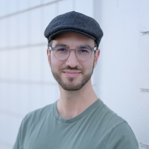
Mark Gottscho, Ph.D.
Computer architect
I am currently a Member of Technical Staff at OpenAI.
My professional interests are in hardware/software codesign of AI chips, agile hardware development methodologies, memory systems, and hardware reliability.
Before joining OpenAI, I was a Senior Manager at SambaNova Systems, where I founded and directed the compiler operators team. Our responsibilities included development of internal MLIR dialects, formalization of operators and mixed precision semantics, and implementation of high performance dataflow kernels. Our work didn’t target GPUs: SambaNova makes a custom AI accelerator chip called the Reconfigurable Dataflow Unit (RDU) that is optimized for both inference and fine-tuning. As the compiler technical lead for a future RDU chip, I drove several hardware/software codesign efforts and bootstrapped a new architecture specification workflow. I invested significant effort into building the engineering culture, growing the team, and speeding up software builds. Outside of work, I moonlighted as a Technical Advisor to ChipStack.ai, a seed-stage startup that is revolutionizing the way chips are designed and verified.
Prior to my work at SambaNova, I was a chip architect, microarchitect, RTL designer, and cross-functional technical lead in Google’s Tensor Processing Unit (TPU) team. All of my projects at Google successfully landed: TPUv4i, TPUv4, TPUv5e, TPUv5p, and Trillium have all been key technologies underlying Google’s AI leadership. My contributions to the TPU spanned most of the subsystems, although the bulk of my impact was on the memory system, host interface, and inter-chip interconnect; I won a Feat of Engineering for my work on the TPUv4 on-chip interconnect. Alongside my co-lead, I landed an internal Chip Development Kit (CDK) from scratch. It is a set of comprehensively specified, parameterizable, and formally verified RTL libraries that implement common dataflow primitives with high performance and minimal area. CDK significantly improved the hardware development velocity and lowered bug rates for several different Google chips (not just TPUs) using a correct-by-construction approach. The vast majority of the gates in recent TPU chips are attributed to CDK modules. It was nominated for a Feat of Engineering.
In 2017, I received my Ph.D. in Electrical Engineering from UCLA for my dissertation titled "Opportunistic Memory Systems in Presence of Hardware Variability." My research explored techniques for exploiting inherent imperfections in hardware to improve energy efficiency, reduce cost, and gracefully recover from errors. In 2016, I won the Qualcomm Innovation Fellowship and the UCLA Dissertation Year Fellowship for my co-invention of "Software-Defined Error-Correcting Codes."
Outside of work, I’m a long-time road racing and sports car enthusiast. Whenever not with my family, you are likely to find me road racing in my Spec E46, simracing online, or enjoying Bay Area backroads.
I’m a dad, husband, son, brother, uncle, and friend.
